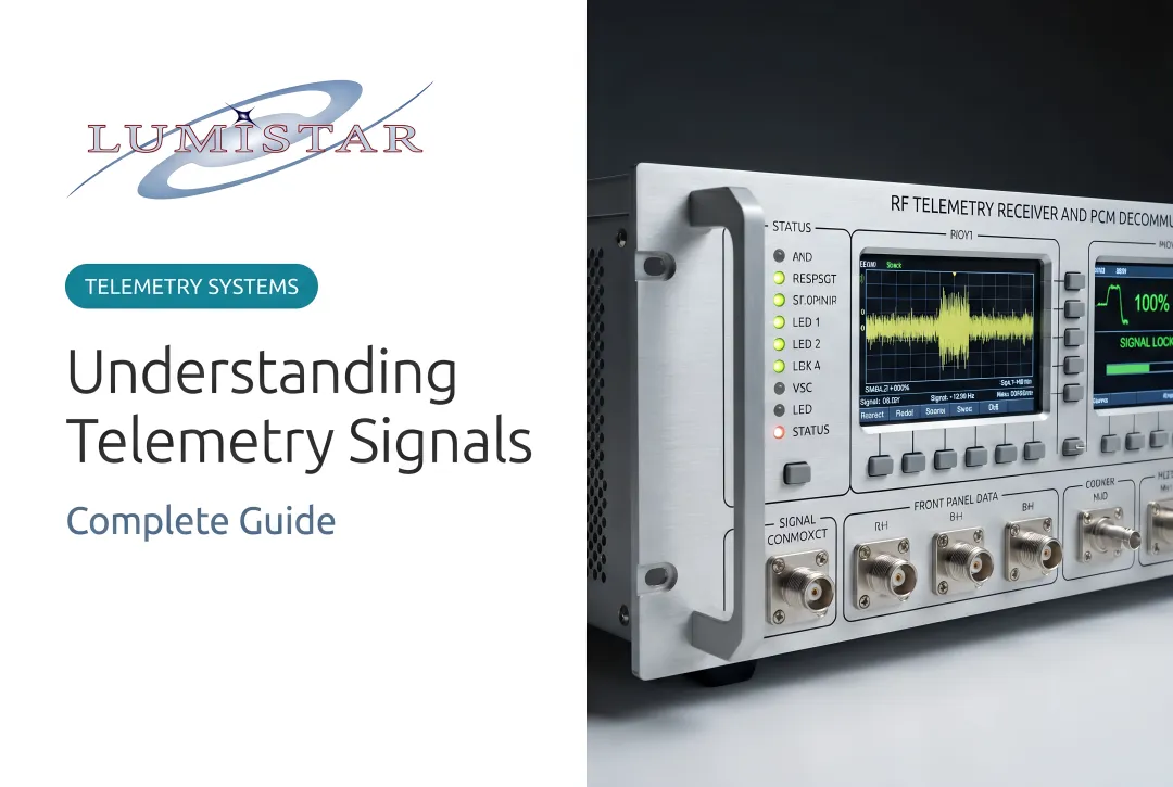
Introduction
RF signals of interest rarely arrive at frequencies that downstream processors can handle directly. A telemetry signal transmitted from a test aircraft might ride a carrier in the L-band at 1.4 GHz — but the demodulator needs baseband data. Something has to bridge that gap.
Traditionally, that job fell to chains of analog mixers, local oscillators, and IF filters. Each stage added noise, component tolerances, and thermal drift. The Digital Down Converter (DDC) replaces most of that analog plumbing with arithmetic, performing frequency translation entirely in the digital domain after the ADC has already sampled the signal.
This article covers:
- What a DDC is and how it works
- How the three-stage processing chain operates
- How DDC compares to analog downconversion
- Why the architecture matters in aeronautical telemetry and flight test systems
Key Takeaways
- A DDC shifts a digitized IF signal to complex baseband (I/Q) without additional analog hardware
- It consists of three stages: NCO (mixer), low-pass filter, and decimator
- Decimation narrows noise bandwidth, improving in-band SNR by 10·log₁₀(M) dB for white noise
- DDCs replace bulky analog IF chains with reconfigurable arithmetic, eliminating hardware changes when retuning
- Implemented in FPGAs or ASICs, they are standard in modern SDR and flight test telemetry receivers
What Is a Digital Down Converter?
A DDC is a DSP block that takes a digitized, band-limited signal at an intermediate frequency (IF) and translates it to a lower center frequency (typically complex baseband I/Q) while simultaneously reducing the output sample rate to match the narrower bandwidth of interest.
Where It Sits in the Signal Chain
The DDC occupies the digital side of the receiver, after the ADC:
- Antenna captures the RF signal
- RF downconverter or direct-sampling ADC digitizes it at an IF (e.g., 70 MHz)
- DDC performs final frequency translation and bandwidth reduction
- Demodulator / data processor receives clean baseband I/Q data
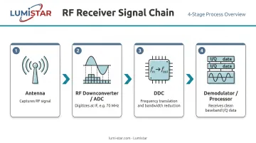
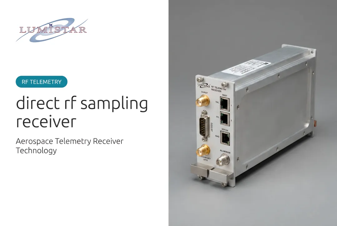
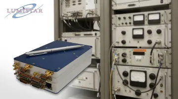
In Lumistar's receiver systems, for example, the LS-35-R IF Receiver processes signals at a standard 70 MHz IF — a fixed reference point that the digital processing stages are built around. The DDC stage inside then handles the translation from 70 MHz to baseband.
DDC vs. Analog Downconversion
Both approaches accomplish frequency translation, but they differ in where and how that work happens:
| Analog Downconverter | DDC | |
|---|---|---|
| Implementation | Physical mixers, oscillators, bandpass filters | Mathematical operations on digitized samples |
| Temperature drift | Yes — components drift and require alignment | No — deterministic digital math |
| Reconfigurability | Requires physical hardware changes | Reprogrammed in firmware or software |
| Consistency | Varies unit to unit | Identical across every run |
Because a DDC operates entirely in the digital domain, it eliminates the calibration overhead and component aging that analog stages introduce.
How a DDC Works: The Signal Processing Flow
A real-valued digitized IF signal enters the DDC. Three operations transform it into usable baseband data:
- Mix — multiply by a complex sinusoid to shift the spectrum down
- Filter — remove the image frequency and out-of-band interference
- Decimate — reduce the sample rate to match the signal bandwidth
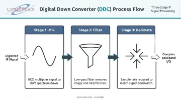
The output is a complex (I/Q) baseband signal. Multiplying a real signal by a complex exponential (e^{j2πft}) produces separate positive and negative frequency components, allowing the filter to retain the desired channel and discard everything else.
This I/Q representation is mathematically equivalent to the original bandpass signal — and it's what demodulators expect.
Mixing with the NCO
The Numerically Controlled Oscillator (NCO) generates a digital complex sinusoid at the chosen tuning frequency. When multiplied sample-by-sample with the incoming digitized signal, the spectrum shifts downward by that frequency (equivalent to analog mixing, but implemented entirely in arithmetic).
Per Analog Devices MT-085, the NCO output frequency follows:
f₀ = M · f_clk / 2^N
where M is the tuning word, f_clk is the clock rate, and N is the accumulator width. Frequency resolution is f_clk / 2^N — a 32-bit accumulator at a 100 MHz clock yields resolution finer than 0.025 Hz.
The NCO tuning frequency must place the signal of interest at or near DC in the output. Poor frequency planning causes the desired signal or its harmonics to alias on top of spurious products after decimation.
Low-Pass Filtering
After mixing, the spectrum contains two things: the desired baseband signal, and an unwanted image at twice the original IF. The low-pass filter passes the baseband signal and rejects everything else.
Filter architecture choices in DDC designs:
| Filter Type | Best For | Key Advantage |
|---|---|---|
| CIC | Large decimation ratios | No multipliers — highly efficient in hardware |
| FIR | Moderate decimation, precise shaping | Linear phase, straightforward design |
| IIR | Low-latency applications | Fewer coefficients, but nonlinear phase |
In practice, CIC and FIR stages are cascaded: the CIC handles coarse, efficient decimation at high sample rates, and a compensation FIR flattens the passband and provides final channel shaping. Lumistar's LS-28-DRSM series, for instance, combines hardware SAW filters with precision digital FIR filters offering over 40,000 selectable IF bandwidths from below 50 kHz to 40 MHz.
IIR filters are less common in DDC paths because their nonlinear phase response can distort modulated signals, a real concern for PCM telemetry demodulation where timing accuracy matters. That phase behavior makes CIC-plus-FIR cascades the practical default before any decimation stage.
Decimation
Decimation (downsampling by integer factor M) reduces the output sample rate from the ADC rate to a lower rate matched to the signal bandwidth. Decimating by 8 turns a 100 MSPS stream into 12.5 MSPS, cutting the computational load on every downstream stage.
Two constraints govern the choice of M:
- The low-pass filter must precede the downsampler — discard samples before filtering and aliasing is inevitable
- The decimated sample rate must remain at least twice the filtered signal bandwidth to satisfy Nyquist
SNR benefit: narrowing the noise bandwidth by factor M reduces in-band noise power. According to Analog Devices, the dynamic range improvement from bandwidth reduction is:
ΔDR = 10 · log₁₀(M) dB
For white noise, each doubling of the decimation ratio yields approximately 3 dB of SNR improvement. Decimate by 16 and you gain ~12 dB. For a weak PCM telemetry signal from a distant test vehicle, that margin can determine whether you recover the data or lose it.
The Three Core Components of a DDC
The Numerically Controlled Oscillator (NCO)
The NCO works through a phase accumulator that increments by a fixed step (the tuning word) each clock cycle. A lookup table or CORDIC algorithm converts the accumulated phase to sine and cosine values, producing the complex sinusoid that drives the mixer.
Key advantages over analog oscillators:
- Tracks the reference clock for frequency stability, eliminating drift from temperature or component aging
- Retunes instantly — update the tuning word register and the output frequency shifts on the next clock cycle
- Delivers fine resolution: a 32-bit accumulator provides sub-Hz precision at typical ADC clock rates
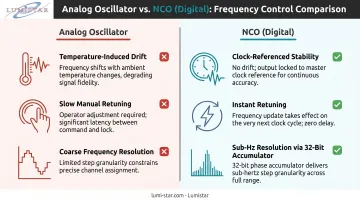
That instant retunability has direct value in flight test applications. Lumistar's LS-18-R1, for example, includes a Doppler shift feature specifically to support tracking moving test vehicles — dynamic frequency adjustment that would require physical LO hardware changes in an analog system.
The Low-Pass Filter
Once the NCO mixer shifts the signal of interest to baseband, the low-pass filter determines what stays and what gets rejected. The CIC+FIR cascade dominates DDC filter design for this stage. The Analog Devices AD9680 illustrates this well: its four integrated DDC channels each use cascaded half-band FIR filters following the NCO mixer stage.
The filter's passband bandwidth directly defines how much spectrum is retained. Its stopband rejection sets the limit on how cleanly adjacent signals are suppressed — a fundamental constraint on selectivity and dynamic range in multi-signal environments.
The Downsampler / Decimator
The downsampler discards M−1 out of every M samples after filtering. Because this step is always preceded by the low-pass filter, engineers treat the two as a single combined "decimation filter" in practice — they're inseparable from a system design standpoint.
Choosing M involves a direct tradeoff:
- Higher M → lower output data rate, better SNR, but narrower useful bandwidth
- Lower M → wider bandwidth retained, but less SNR improvement and higher downstream data rate
The governing principle: output sample rate ≥ 2 × filtered signal bandwidth (Nyquist). Violate this and the signal aliases onto itself, destroying information.
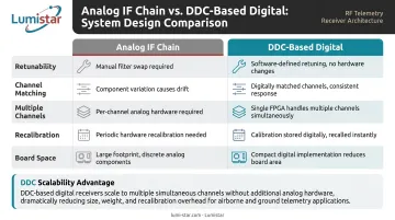
DDC vs. Analog Downconversion: Key Differences
A multi-stage analog IF chain involves physical mixers, local oscillators, bandpass filters, and amplifiers at each frequency conversion step. Each component introduces:
- Gain variation over temperature and frequency
- Phase noise from the local oscillator
- Component tolerance mismatches between channels
- Periodic recalibration requirements
DDC eliminates most of this by replacing analog stages with deterministic arithmetic — once digitized, all frequency translation and filtering are fixed, repeatable math. Texas Instruments' RF-sampling research demonstrated that advancing ADC technology allows removal of the last analog downconversion stage entirely, with the DDC handling what analog mixers previously did. The table below shows how this plays out across common system design concerns.
Practical System Implications
| Aspect | Analog IF Chain | DDC-Based Digital |
|---|---|---|
| Retunability | Replace/adjust hardware | Change a register value |
| Channel matching | Component tolerances apply | Identical arithmetic for all channels |
| Multiple simultaneous channels | Requires duplicate analog hardware | Multiple DDC instances share one ADC |
| Recalibration | Periodic, temperature-driven | Not required |
| Board space | Grows with channel count | Scales in FPGA fabric |
Running multiple DDC instances from a single ADC is one of the most practical advantages for flight test applications. Lumistar's LS-29-R2 RF Recording system supports two or four independent DDC channels simultaneously, each processing up to 50 MHz of instantaneous bandwidth from a single wideband digitized stream. That covers up to 200 MHz of RF spectrum across a 200 MHz to 6 GHz range.
Benefits and Applications in Telemetry and Aerospace Systems
DDC architecture delivers a specific set of engineering advantages that align directly with what flight test telemetry demands:
- Improved SNR via decimation filtering — critical for weak signals from distant test vehicles
- Flexible channel tuning — change the NCO tuning word to switch bands without touching hardware
- Elimination of analog drift — all-digital processing maintains consistent performance over temperature
- Reduced SWaP (Size, Weight, and Power) — FPGA-based DDC replaces multiple analog stages
- Multiple virtual receivers from one digitized stream — simultaneous multi-link reception
These benefits translate directly into modern flight test ground station design. The IRIG-106 standard, maintained by the Range Commanders Council, governs aeronautical telemetry interoperability across RCC member ranges and specifies receiver requirements including standard IF bandwidths of 300 kHz, 1 MHz, and 20 MHz — with additional bandwidths noted for receivers using digital IF filtering.
Those IRIG-106 requirements shaped Lumistar's development path directly. Less than 20 years ago, a typical telemetry ground station stood 8 feet tall, weighed 250 kg, and consumed thousands of watts. Lumistar's current LS-28-DRSM series, a fourth-generation software-defined radio platform with dual-channel DSP architecture, fits in a unit measuring 6" × 4" × 1.67", weighs under 1 kg, and runs on 40 watts.
The LS-28-DRSM supports over 40,000 automatically optimized IF bandwidths and tuner resolution down to 1 Hz, reconfigurable entirely through firmware without hardware changes.
Moving the signal processing workload into FPGA fabric through DDC architecture is what made that reduction in size, weight, and power achievable — without sacrificing receiver performance.
Frequently Asked Questions
What does a down converter do?
A down converter shifts a high-frequency signal to a lower frequency for easier processing. In DSP, a digital down converter does this mathematically on sampled data — translating a digitized IF signal to baseband so demodulators and data processors can operate without needing additional analog hardware.
How does a digital down converter work?
The process runs in three stages. An NCO generates a digital sinusoid at the signal's center frequency; the incoming digitized signal is multiplied by this sinusoid to shift the spectrum to baseband; then a low-pass decimation filter reduces the sample rate to match the signal bandwidth while improving SNR.
When do you use a downconverter versus an upconverter?
In receiver applications, you need a downconverter — moving a signal from IF to baseband for demodulation. An upconverter does the opposite, preparing a baseband signal for transmission at a higher carrier frequency. Almost all receive-chain applications require downconversion.
What is decimation in a digital down converter?
Decimation reduces the sample rate by discarding samples at a fixed ratio after low-pass filtering. This lowers data throughput to downstream processors and narrows the noise bandwidth, improving the signal-to-noise ratio within the band of interest by approximately 10 × log₁₀(M) dB.
How is a DDC typically implemented in hardware?
DDCs are most commonly implemented in FPGAs or ASICs, which execute NCO, multiplication, and filter operations at full ADC sample rates. Many modern RF ADC chips integrate DDC blocks directly, such as the TI ADC12DJ3200QML-SP, a 6.4 GSPS device with optional on-chip DDCs. Lumistar implements DDC functions in Xilinx Virtex-5 FPGA arrays within its receiver products.